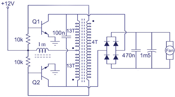
Booster circuit and inverter topology with cascade diode circuit Circuit Diagram
Booster circuit and inverter topology with cascade diode circuit Circuit Diagram There are 2 circuits used in a boost converter. The boost circuit- It has an inducter, a switch, a diode and a capacitor. A quick change in current through the inducter due to the switch results in a huge voltage across it. This huge voltage creates a huge current which charges up the capacitor. The diode doesn't let the capacitor discharge
A Practical Boost Converter Circuit Design using IC 555 Now let's refer to our fourth step-up converter design which will boost a 3.7 V input DC to 24 V output DC. This simple circuit is built using an IC 555 circuit for boosting USB 5V to 24V , or any other desired level. Design of the Adjustable VOUT Boost Circuit Application Report SLVAEJ4-December 2019 Design of the Adjustable VOUT Boost Circuit RobinLiu ABSTRACT This application note introduces a method to design an adjustable or programmable output voltage for a boost converter. The circuit implementation and design procedure are discussed in detail. Contents
Introduction to the Boost Converter: Structure and Design Circuit Diagram
We design a boost converter circuit based on timer IC 555 and a few easy-to-available external components. In this boost converter circuit, IC 555 is configured in Astable multivibrator mode and we can adjust the output voltage by varying the output pulse frequency of the timer IC. Now I'll create a boost converter design for LTspice. As with the LTspice buck converter, I'll use a voltage-controlled switch instead of a transistor. My implementation is below, in Figure 2: it represents a circuit intended for low-voltage, battery-powered applications, and the values I've chosen reflect this.

Proper design of the inductor is the cornerstone of a good boost design as well as any other switching power supply. When the inductor has the proper inductance and can handle the peak and RMS currents over the full range of V-in and V-out, especially taking into account the frequency of the circuit, then everything else tends to fall into place.

Boost Converter Circuit using 555 Timer IC Circuit Diagram
In reality, the design and testing of a boost converter is a lot easier than meets the eye. Here I will walk you step by step on designing your first boost converter and how the datasheet is your best friend when designing. For this tutorial we will be using the L6920DC IC Boost converter from skyworks. [1] A DC Voltage booster circuit boosts a low-level DC signal, namely 1.5V to 3V to a significantly higher DC level. they commonly serve in applications requiring a much higher DC power input (about 60V to 80V DC). So, in this project, we are going to design a simple & inexpensive voltage booster circuit using transistors.